- 您现在的位置:买卖IC网 > Sheet目录39249 > LM7001JM PLL FREQUENCY SYNTHESIZER, 130 MHz, PDSO20
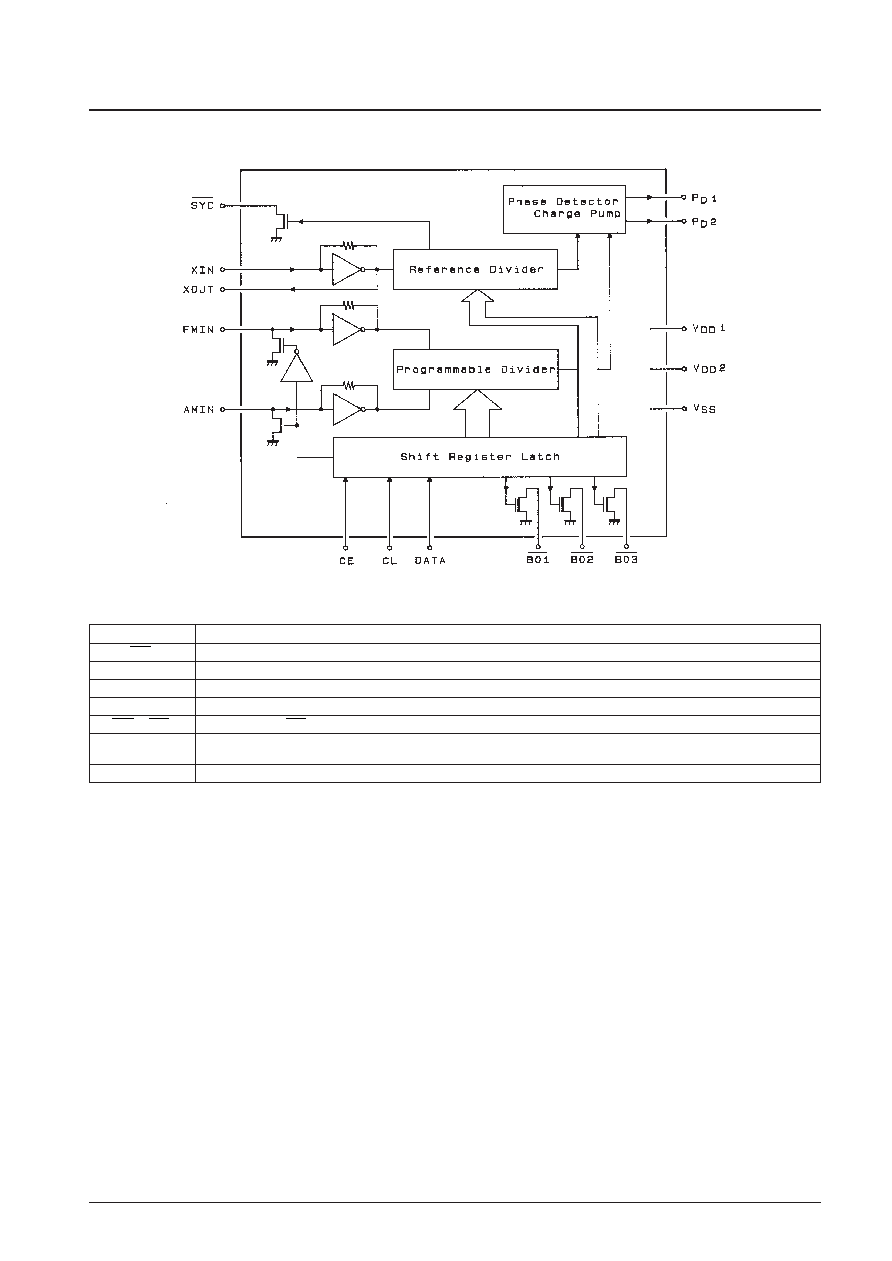
Equivalent Circuit Block Diagram
Pin Functions
No. 5262-4/8
LM7001J, 7001JM
Symbol
Description
SYC
Controller clock (400 kHz)
XIN, XOUT
Crystal oscillator (7.2 MHz)
FMIN, AMIN
Local oscillator signal input
CE, CL, DATA
Data input
BO1 to BO3
Band data output. BO1 can be used as a time base output (8 Hz).
VDD1, VDD2, VSS
Power supply (Apply power to both VDD1 and VDD2 when the PLL circuit is operating. VDD2 is the crystal oscillator and time base
power supply. Internal data cannot be maintained on VDD2 only.)
PD1, PD2
Charge pump output
发布紧急采购,3分钟左右您将得到回复。
相关PDF资料
LM7001M
PLL FREQUENCY SYNTHESIZER, 130 MHz, PDSO20
LM7006
PLL FREQUENCY SYNTHESIZER, 400 MHz, PDIP20
LM7006H
PLL FREQUENCY SYNTHESIZER, 400 MHz, PDIP20
LM7007M
PLL FREQUENCY SYNTHESIZER, 520 MHz, PDSO24
LMC500-5SS
LOW PASS FILTER
LMC500-5SM
LOW PASS FILTER
LMC500-5SL
LOW PASS FILTER
LMC500-5SB
LOW PASS FILTER
相关代理商/技术参数
LM7001M
制造商:未知厂家 制造商全称:未知厂家 功能描述:Direct PLL Frequency Synthesizers(256.46 k)
LM7001R
制造商:Panasonic Industrial Company 功能描述:IC
LM7005
制造商:SANYO 制造商全称:Sanyo Semicon Device 功能描述:Electronic AV Tuner-Use Electronic Tuning PLL Frequency Synthesizer
LM7006
制造商:SANYO 制造商全称:Sanyo Semicon Device 功能描述:Dual PLL Frequency Synthesizer Circuit
LM7006H
制造商:SANYO 制造商全称:Sanyo Semicon Device 功能描述:Dual PLL Frequency Synthesizer Circuit
LM7007HM
制造商:SANYO 制造商全称:Sanyo Semicon Device 功能描述:Dual-PLL Frequency Synthesizers
LM7007M
制造商:SANYO 制造商全称:Sanyo Semicon Device 功能描述:Dual-PLL Frequency Synthesizers
LM7008
制造商:SANYO 制造商全称:Sanyo Semicon Device 功能描述:Dual-PLL Frequency Synthesizers